- PCB Design for Rugged Environments
- PCB Material Selection for Ruggedized Circuit Board Design
- Component Placement and Mounting for Vibration Resistance
- Outdoor PCB Design Best Practices
- Testing PCB Design for Harsh Conditions
- Building Rugged Electronics Without Slowing Innovation
Best Practices for PCB Design in Rugged Environments
Designing electronics to survive the real world is challenging. Conditions change, equipment vibrates and moisture finds its way into places it shouldn’t.
A board may perform well in testing but struggle once it moves into production or deployment. Rugged PCB design reduces that risk by shifting the focus from reactive to proactive. That means thinking carefully about materials, layout, mechanical support, environmental protection and how to validate the board before releasing it.
These PCB design best practices let you create boards that hold up under stress while keeping development timelines realistic and manageable.
PCB Design for Rugged Environments
Rugged PCB design starts with understanding the conditions the board will face during daily operation. The environment shapes material choices, layout decisions and protection strategies.
Designing a Vibration-Resistant PCB for Automotive and Industrial Applications
Vibration introduces continuous mechanical movement. Over time, that movement can weaken solder joints, shift connectors and create stress around heavier components.
Approaches for a vibration-resistant PCB include the following.
- Board support strategy: Placing mounting points near heavier areas reduces flex during operation.
- Component profile control: Lower profile components move less and place less strain on solder joints.
- Balanced layout: Distributing mass across the board prevents localized stress.
Coping With Extreme Temperature Fluctuations and Thermal Shock
Temperature changes cause materials to expand and contract at different rates. Repeated cycling can lead to fatigue in solder joints, layer delamination and gradual performance degradation.
Temperature-resistant PCB design often involves selecting materials with compatible thermal properties and managing how heat moves across the board.
Resisting Moisture, Dust and Chemical Contaminants
Environmental exposure affects reliability in quieter ways. Moisture can lead to corrosion, dust can create leakage paths and chemical exposure can degrade protective layers.
Outdoor and industrial designs typically account for this through sealing strategies, protective coatings and connector choices that limit ingress without making the system difficult to service.
Understanding these environmental factors early makes later design decisions more intentional and reduces the likelihood of redesign.
PCB Material Selection for Ruggedized Circuit Board Design
Material influences how well a board holds up over time. Of course, electrical performance matters. However, mechanical stability and thermal behavior are central to reliability in harsh conditions.
The goal is to prevent issues that are difficult to correct later, such as warping, solder fatigue or layer separation.
High-Tg FR4 vs. Polyimide
High-Tg FR4 remains a common choice because it offers improved thermal stability compared to standard FR4 while maintaining cost efficiency. For many industrial applications, it provides a practical balance between performance and manufacturability.
Polyimide becomes more relevant when boards must tolerate higher temperatures, repeated thermal cycling or increased mechanical stress. Its flexibility and thermal resistance make it useful in designs where standard materials may fatigue over time.
Consider these material selection variables.
- Thermal range: Higher glass transition temperatures support more stable operation during temperature cycling.
- Mechanical behavior: Materials that resist cracking or flex fatigue extend product life.
- Production scale: Some materials introduce longer lead times or additional manufacturing considerations.
Copper Weight and Plating Thickness for Durability
Copper structure influences electrical performance and mechanical strength. Heavier copper can improve current handling and reduce localized heating, while thicker plating strengthens pads and vias that experience stress.
Durable PCB design involves:
- Increased copper weight for power distribution.
- Reinforced vias in high-stress areas.
- Plating strategies that reduce fatigue over time.
Component Placement and Mounting for Vibration Resistance
In rugged environments, component placement influences how the board handles movement, stress and long-term fatigue. A stable layout reduces the load placed on solder joints and connectors. It also makes validation more predictable because the board behaves consistently under vibration and mechanical shock.
Strategic Component Layout to Minimize Flex Stress
Boards naturally flex during operation, especially in vibration-heavy applications. Placement determines flex distribution. Design teams often focus on:
- Positioning heavier components near mounting points
- Avoiding high-mass clustering
- Keeping sensitive components away from board edges
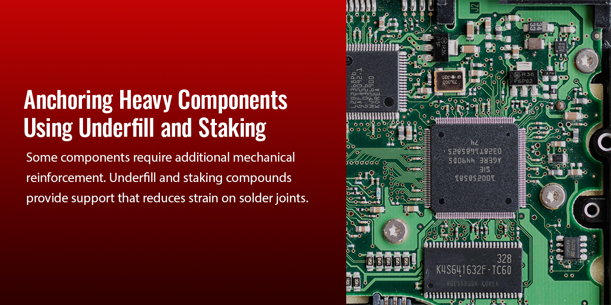
Anchoring Heavy Components Using Underfill and Staking
Some components require additional mechanical reinforcement. Underfill and staking compounds provide support that reduces strain on solder joints. These methods apply to connectors, large capacitors and components exposed to continuous vibration. They distribute stress more evenly and extend service life.
Selecting Rugged Connectors and Locking Mechanisms
Connectors experience repeated movement during operation and maintenance. Standard connectors may loosen over time, leading to intermittent failures that are difficult to diagnose.
Trace Routing and Thermal Management Strategies
Routing decisions influence more than signal integrity. In rugged applications, trace design affects heat distribution, mechanical durability and how the board responds to repeated stress.
Thermal buildup and localized stress often appear gradually. Routing that supports even heat flow and avoids vulnerable areas maintains performance over time. The objectives are consistency, stable temperatures, predictable current paths and reduced stress on critical interconnects.
Designing Power Planes for Effective Thermal Dissipation
Power planes spread heat across a larger area, preventing it from concentrating around individual components. It reduces thermal gradients that can accelerate material fatigue.
Strategies include:
- Using larger copper areas to improve heat spreading and reduce hot spots.
- Adding thermal vias beneath high-power components to move heat into inner layers.
- Planning stackups with thermal behavior in mind for cooling and mechanical stability.
Trace Widths and Via Protection in High-Stress Zones
Trace geometry changes as boards flex and vibrate. Narrow traces are more susceptible to cracking, particularly near connectors or mounting areas. Designers often address this by increasing trace width in critical pathways, routing away from known flex zones and protecting vias through tenting or filling.
Outdoor PCB Design Best Practices — Protective Coatings and Enclosure Integration
In rugged applications, PCB design and enclosure strategy need to work together. Moisture, dust and chemical exposure don’t always cause immediate failure. The damage often builds slowly.
Conformal Coating and Potting for Environmental Sealing
Conformal coating creates a thin protective layer that shields board components and traces from moisture and contaminants while keeping the assembly serviceable. Potting provides superior protection by encapsulating components in a compound. It improves vibration resistance and environmental exposure but limits repairability.
Design Considerations for Sealed Enclosures
A sealed enclosure adds another layer of defense, but it also introduces thermal and pressure considerations. Internal heat buildup can shorten component lifespan if not managed correctly.
Design teams often coordinate on:
- Ventilation or pressure equalization strategies
- Gasket and sealing material selection
- Mechanical support alignment
Testing PCB Design for Harsh Conditions
Validation confirms that design assumptions hold under real-world conditions. Early testing reduces the risk of field failures and redesign cycles.
Thermal Cycling and HALT HASS Testing Protocols
Thermal cycling evaluates material fatigue, while accelerated testing methods expose hidden weaknesses earlier in development. These approaches are common in ruggedized and mil-spec PCB design contexts, where reliability requirements are higher.
The Importance of Solder Paste Inspection for Joint Reliability
Solder paste inspection verifies paste volume and placement before reflow, improving solder joint consistency. Reliable joints are critical for vibration resistance and long-term durability, making SPI essential in rugged electronics manufacturing.
Building Rugged Electronics Without Slowing Innovation
Designing electronics for harsh environments means managing uncertainty. Engineers must deliver reliable products while working within tight schedules, complex supply chains and evolving performance expectations.
Thoughtful material selection, layout strategies, environmental protection and validation methods let teams create electronics that perform consistently in demanding conditions. It’s equally crucial to work with partners who understand engineering and production to reduce friction throughout development and protect time-to-market.
If you develop rugged electronics and want to streamline design, prototyping and production within a single integrated workflow, request a quote from Lectronix today and explore how a coordinated engineering and manufacturing approach can support reliable product development.