Testing and Validation Strategies for Automotive Electronics
Modern vehicles rely on distributed electronics, tight software integration and safety-critical control logic. That complexity makes automotive electronics testing and vehicle electronics validation essential for reliability, compliance and time-to-market. At Lectronix, we help engineering teams de-risk launches by building test plans that scale from component verification to full platform validation, with clear documentation, repeatable processes and actionable results, enabling faster decisions.
The Cost of Gaps in Validation
When components are developed by multiple vendors, the internal engineering team still has to bring those pieces together into a single working system. At each stage, from design and prototyping to verification, the team needs a clear validation framework for the deliverables coming from each partner.
Without that framework, defects may not surface until late in the process. A missed issue in one component can trigger re-spins, schedule delays and repeat development work across other parts of the program. A structured validation approach helps catch defects earlier, reduce costly rework and support consistent decision-making across engineering and manufacturing.
A Framework for Comprehensive Automotive Quality Assurance
High-reliability programs work best when testing is staged and intentional. A complete framework typically includes unit, integration and system-level verification in addition to standards-driven compliance testing. Below is a practical structure used in many advanced electronics programs.
Foundational Automotive Hardware Testing and Integration
Start by verifying both the build quality and performance of individual boards, harnesses and firmware modules before the system is assembled. Manufacturing process checks, such as Solder Paste Inspections (SPI), can help confirm production quality before functional testing begins. This is where ECU testing and automotive functional testing help confirm I/O behavior, sensor inputs and control outputs under expected operating conditions. Integration testing then validates communication between modules, ensuring interfaces behave correctly before you commit to full builds.
Vehicle System Validation and Reliability
As subsystems come together, validation shifts to the full platform. Vehicle system validation verifies end-to-end behavior in realistic scenarios, including fault handling and edge cases. Environmental and reliability testing support durability by evaluating performance under temperature extremes, vibration and moisture, which can affect electronics over time.
Safety and Compliance Testing of Automotive Requirements
For safety-related systems, alignment with standards is not optional. ISO 26262 is a core functional safety framework used across road vehicle programs. It informs how teams plan for hazards, define safety goals and verify the software and hardware behaviors associated with risk. By compliance testing automotive electronics, you can tie evidence back to requirements, so approvals are faster and defensible.
Why Trust Us?
We do not treat validation as a last-minute checklist. At Lectronix, we build testing plans that protect your launch window by aligning requirements, engineering and manufacturing early. From our Michigan-based engineering and production teams, we support design verification, prototyping and test execution under one roof, reducing handoff delays and clarifying ownership.
We use proven inspection and process controls, including Solder Paste Inspection, to support build quality. Our quality management system is certified to the IATF 16949 automotive standard, and our teams are accustomed to high-reliability programs across defense and industrial automation. The result is a clearer path to validation and fewer surprises late in the schedule.
Move Faster With a Single Technical Partner
If you need a team that can execute testing and validation while supporting design and build readiness, Lectronix can help. Learn more about our engineering services or request a quote to discuss your program requirements and timeline.
Embedded Software Development: Common Pitfalls and Solutions
Embedded systems development requires balancing real-time performance requirements, memory constraints and tight timelines while maintaining the precision needed to deliver stable, market-ready products. Teams understand that process decisions and coding practices determine whether a system performs reliably in the field or requires costly troubleshooting.
The key is identifying which strategies prevent common failures rather than simply addressing them after they occur. This guide covers proven approaches to embedded software development, from establishing sound project frameworks to implementing coding practices to eliminate errors that threaten product launches.
High-Level Process Pitfalls That Derail Projects
Technical failures in real time embedded software may trace back to flawed processes and inadequate project planning. These high-level mistakes become embedded in the product architecture before development begins, creating conditions for scope creep, repeated rework, field failures and delayed launches.
Recognizing common embedded development mistakes early allows teams to establish frameworks that prevent problems rather than manage them after they emerge.
Inadequate Requirements and Unclear Specifications
Vague or incomplete requirements create conditions for constant scope adjustments, mismatched features and expensive late-stage changes. Without a detailed, stakeholder-approved product requirements document (PRD), development teams spend resources building functionality that does not align with actual product goals.
Clear specifications establish the boundaries within which engineering decisions can be made confidently. Information in the PRD should include:
Memory limits.
Real-time constraints.
Power budgets.
Regulatory needs.
Overengineering and Feature Creep
Adding unplanned complexity or unnecessary features consumes limited memory and processing power while multiplying potential failure points. This approach diverts resources from core functionalities and increases the risk of system instability. Maintaining discipline around the defined feature set protects both timeline and system reliability.
Insufficient Testing and Validation Strategies
Relying on manual, late-stage testing misses hardware-specific issues. A continuous, multilayered testing strategy that includes automated regression testing and hardware-in-the-loop validation catches integration issues early, when they’re less expensive to resolve. Testing frameworks built into the development process provide consistent feedback throughout the build cycle.
Neglecting Documentation and Long-Term Maintainability
Poor or missing documentation turns long-lifecycle industrial and automotive products into maintenance challenges. Bug fixes, firmware updates and onboarding new engineers become slow and expensive when original design decisions are not captured clearly. Comprehensive documentation protects the product investment and enables efficient support from product development to launch.
Critical Low-Level Coding Pitfalls That Cause System Failures
While process mistakes create conditions for failure, direct coding errors can trigger crashes, memory faults, freezes and watchdog resets that halt development and delay product releases.
Memory Management Mishaps
Embedded systems operate under strict memory constraints that make allocation errors particularly damaging. Incorrect dynamic allocation without proper supervision causes fragmentation, leaks and overflows.
Failing to free resources or using uninitialized memory can lead to runtime errors that may only surface under extended operation or specific usage patterns. Stack overflows from deep recursion or large local variables create equally serious stability problems that compromise system reliability.
Real-Time Processing and Timing Errors
Real-time embedded software demands precise timing to meet system requirements. Blocking functions or lengthy interrupt service routines cause system hangs, missed deadlines and data loss that violate real-time constraints.
Polling loops waste processor cycles and introduce timing jitter that degrades performance predictability. Efficient task scheduling and interrupt management are necessary to maintain the deterministic behavior that real-time systems require.
Ignoring Hardware and Compiler Behavior
Compiler optimizations can cache values from hardware registers, creating silent bugs that are difficult to trace. For example, omitting the volatile keyword on memory-mapped registers or shared variables is a common cause of intermittent failures.
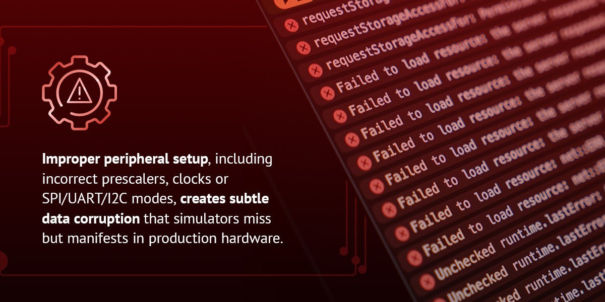
Improper peripheral setup, including incorrect prescalers, clocks or SPI/UART/I2C modes, creates subtle data corruption that simulators miss but manifests in production hardware. Understanding how the compiler and target hardware interact prevents these low-visibility errors.
Overlooking Security Vulnerabilities From the Start
Security weaknesses cannot be addressed effectively after initial development. Buffer overflows, improper pointer use and weak error handling in connected systems create exploitable entry points.
In industrial and automotive applications, these vulnerabilities can compromise both safety and data integrity, making early security design a functional requirement rather than an optional enhancement.
Best Practices for Delivering Robust Embedded Systems
Proven strategies eliminate the pitfalls in processes and coding and support stable, market-ready embedded software best practices. These approaches create consistency across builds and reduce the variability that extends timelines.
Adopting a Structured Development Life Cycle
Methodologies like the V-Model or Agile adapted for embedded systems create a formal framework for requirements, design, implementation and testing.
This disciplined approach supports firmware development capabilities across real-time systems on 8/16/32-bit platforms, real-time operating systems (RTOS) environments, low-level drivers, interrupt handlers, device drivers, GUI creation and full-lifecycle support from concept through manufacturing. Structured processes ensure that each development phase receives appropriate attention and validation.
Implementing Rigorous, Automated Testing
Automated testing integrated into a continuous integration and deployment pipeline replaces unreliable, late-stage manual testing with consistent, repeatable validation for every code change.
Hardware-in-the-loop testing runs actual firmware on target hardware, catching pin interference, propagation delays, peripheral timing issues, physical PCB errors and environmental effects that simulators struggle to reproduce. This approach can help reduce the chances of post-deployment failures and enable reliable embedded software debugging throughout development, reducing the cost and timeline impact of defects discovered late.
Enforcing Strict Coding Standards
Strict coding standards such as MISRA C prevent many low-level errors, including uninitialized variables, unsafe pointer use and improper type conversions. MISRA C originated in the automotive industry in 1998 and remains the benchmark for safety-critical embedded C programming.
The current edition, MISRA C:2025, provides rules that improve code safety, security, portability and long-term maintainability in industrial and automotive applications where reliability directly affects product success.
Bridging the Gap Between Hardware and Software Teams
Tight, continuous collaboration between hardware engineers and software engineers from the first prototype forward prevents integration failures. Early communication ensures that firmware is fully optimized for the actual microcontroller architecture, memory constraints and real-time requirements.
Joint reviews of schematics, pin assignments, timing diagrams and peripheral behavior eliminate the disconnect that causes most hard-to-debug embedded systems programming issues. When both teams understand the full system context, design decisions support rather than complicate implementation.
Get Started With Lectronix, Inc.
Reliable embedded software depends on disciplined planning, careful firmware design and real-world validation before deployment. When teams miss early problems or treat hardware and software as separate workflows, small defects can turn into unusable products.
Lectronix, Inc. helps engineering teams avoid those risks with full-lifecycle embedded systems support, from early architecture through firmware development, driver integration, testing, and manufacturing readiness. Our team has extensive expertise with real-time systems, low-level software, hardware-aware development and safety-focused coding practices that help products perform reliably in any environment.
Request a quote today to start building embedded software that’s stable, maintainable and ready for the real world.
New Product Introduction: Timeline and Best Practices
Product launches succeed when engineering leaders balance speed with disciplined process controls. A structured new product introduction (NPI) process enables companies to get products to market faster while maintaining quality standards and cost targets at every phase gate.
The framework embeds risk management and validation checkpoints directly into development cycles, creating predictable launch timing that protects product integrity and competitive advantage.
When market windows shrink and product life cycles compress, the ability to move from concept to volume production with minimal adjustments determines which companies capture early market share.
Why a Disciplined NPI Process Is a Competitive Advantage
A disciplined NPI process is a strategic priority that delivers predictable timelines, controlled costs and superior quality for complex electronics. Speed matters because companies that launch first in a product category capture disproportionate market share before competitors can respond.
A structured product introduction strategy creates a competitive advantage by enabling faster market entry while maintaining the technical rigor that ensures long-term product reliability.
How Time to Market Directly Impacts Profitability
Launch delays cut directly into lifetime profitability, with revenue and margin losses compounding as schedules slip. Shorter time-to-market for products reduces development costs by limiting resources during extended engineering cycles while enabling earlier access to customer revenue.
The advantages of speed become particularly valuable in shrinking product life cycles, where speed as a competitive factor determines market share distribution across an entire category. Companies that can shorten the product development timeline without sacrificing quality capture premium pricing windows and establish brand positioning before competitors can launch alternative solutions.
The Hidden Costs of a Disconnected NPI Process
Many life cycle costs lock in during the design phase. Disconnected NPI efforts can trigger budget overruns through expensive rework cycles, excess inventory accumulation and extended lead times that delay revenue recognition.
Field failures from inadequate validation damage brand reputation and erode customer confidence, creating costs that persist long after the initial launch. Engineering teams working across fragmented vendor networks face communication breakdowns that multiply error rates and extend troubleshooting time.
Errors in the design phase convert what should be predictable development into reactive problem-solving that consumes resources and delays market entry.
The Lectronix NPI Step-by-Step Framework
A proven phase-gate NPI framework moves electronics products from design release to full-scale production while minimizing risk at each transition. Each phase includes clear deliverables, defined timelines, risk gates and resource assignments that maintain continuity from prototype to mass production.
The structured approach to NPI best practices ensures cross-functional teams remain aligned on technical requirements and schedule commitments throughout the product development timeline.
Phase 1: Concept Design and Feasibility
A dedicated program manager joins customer teams at design release to ensure complete documentation, tooling plans and test strategies are in place before hardware development begins.
Engineering teams perform detailed Design for Manufacturability (DFM) analyses that identify potential production constraints. They then create the Product Requirements Document (PRD) that locks specifications and conduct market analysis within four to eight weeks.
Phase completion confirms material choices, component availability and manufacturability requirements before committing resources to prototype builds.
Phase 2: Development and Prototype Validation
In-house hardware, software and mechanical engineering teams build functional prototypes using a complete Bill of Materials (BOM) and Computer-Aided Design (CAD) models.
End-to-end electronic product development capabilities enable rapid iteration cycles across eight to 12 weeks, with multiple design reviews ensuring alignment between customer requirements and technical implementation.
An Engineering Validation Test (EVT) and reliability testing confirm the product meets all technical and quality gates before advancing to production validation.
Phase 3: Production Validation and Process Controls
Suppliers undergo capability audits and sample validation, and manufacturing processes are developed and documented to ensure repeatability at scale. A Design Validation Test (DVT) freezes the design by confirming all specifications perform as intended. A Production Validation Test (PVT) proves the product can be built reliably during a 6- to 10-week phase.
Pilot builds establish process capability metrics, quality plans and yield targets that define acceptable performance ranges for repeatable manufacturing operations.
Phase 4: Manufacturing Ramp-Up and Launch
Production scales over eight to 16 weeks through line balancing and process monitoring that deliver steady-state output. Turnkey manufacturing services integrate functional testing and quality control at every production stage, ensuring target cost and quality levels remain stable as volumes increase.
The program manager oversees the full transition to ensure zero loss of continuity into volume manufacturing, maintaining technical documentation and process knowledge throughout ramp activities.
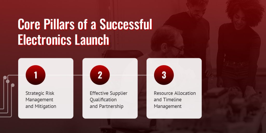
Core Pillars of a Successful Electronics Launch
Successful electronics launches rest on three integrated pillars within the product introduction strategy that ensure speed, quality and cost control across development and production phases.
Strategic Risk Management and Mitigation
Risks are identified at every phase-gate review using formal risk matrices and Design Failure Mode and Effects Analysis (DFMEA) that quantify potential failure impacts. Early mitigation strategies and regular Key Performance Indicator (KPI) tracking keep programs on schedule by turning potential problems into actionable items before they affect timelines.
Cross-functional status updates maintain visibility across engineering, supply chain and manufacturing teams, ensuring resource allocation adjusts dynamically as program requirements evolve.
Effective Supplier Qualification and Partnership
Suppliers are qualified based on their production capacity, quality control systems and technical competence before purchase orders are issued. Sample validation and ongoing performance scoring create accountability that drives continuous improvement in delivery reliability and component quality.
Close collaboration with qualified suppliers secures reliable material flow and reduces lead times. Solid supplier relationships also enable cost optimization initiatives that improve margins without compromising quality standards.
Resource Allocation and Timeline Management
Cross-functional teams receive clear phase plans with assigned owners and realistic timelines that account for validation cycles, supplier lead times and process development requirements. Weekly progress reviews and real-time tracking tools maintain alignment while surfacing constraint issues before they affect the schedule.
Leveraging proven building-block technologies accelerates development by reusing validated designs and processes, reducing risk while speeding up the product launch timeline.
Evaluating an NPI Manufacturing Partner
Engineering leaders who outsource NPI need practical criteria to select manufacturing partners capable of executing complex electronics programs. Successful companies choose partners based on proven process capability and execution track records.
Key Criteria for Partner Selection
Leading manufacturing partners maintain in-house design review, prototype validation and processes that eliminate handoff delays between engineering and production teams. Scalable production capacity ensures that facility limitations or equipment availability don’t constrain the schedule.
Strong on-time delivery performance supported by IATF 16949 and ISO 9001 quality systems demonstrates the process discipline required to maintain schedule commitments and quality standards simultaneously.
Questions to Ask a Potential Partner
Evaluating partner capabilities requires direct questions about process rigor and execution experience. Ask potential suppliers the following:
How do you perform DFM and DFT analysis during the design release phase? Partners should demonstrate structured review processes that identify manufacturability issues before prototyping begins.
What is your average timeline from prototype validation to full production ramp-up? Realistic timelines reflect process maturity and resource availability, while overly aggressive estimates signal a potential schedule risk.
How do you qualify suppliers and manage supply-chain risks throughout the NPI process? Supplier qualification depth directly impacts component quality and delivery reliability across production volumes.
Can you share recent case studies of similar electronics programs you have supported before? Relevant experience in comparable product categories reduces learning curves and execution risk.
Launch Your Next Product With Lectronix, Inc.
Disciplined NPI execution delivers measurable advantages in speed, cost containment and product reliability across every phase from concept validation through manufacturing ramp-up. Choosing the right partner is a critical part of speeding up time-to-market and capturing market share before competitors.
Lectronix, Inc. integrates engineering, prototyping and production under one U.S.-based operation, eliminating the handoff delays and specification drift common in programs with multiple vendors. Our dedicated program managers maintain continuity throughout, ensuring zero loss of institutional knowledge during phase transitions. We protect market windows by accelerating development cycles without sacrificing quality or creating technical debt that surfaces after launch.
Request a quote for expert guidance on NPI best practices or tailored solutions that turn electronics concepts into market-ready products.
Product launches carry pressure long before anything ships. Engineering teams are balancing timelines, performance requirements, supplier coordination and the constant concern that a minor manufacturing issue could create a much larger problem later.
In printed circuit board (PCB) assembly, that risk often comes from defects that are difficult to see early. A slight variation in solder paste or a component that shifts during placement can lead to rework, delayed validation, field failures and uncomfortable conversations about reliability. Teams know quality control matters. The challenge is understanding which measures actually prevent defects rather than simply catching them after the fact.
Below, we discuss the quality control measures used in PCB assembly to reduce risk across the build process. We also cover AOI automated optical inspection, functional testing, solder joint quality assessment, defect-prevention strategies, and statistical process control methods, so teams can make more confident manufacturing decisions.
Why PCB Assembly Quality Control Standards Matter
PCB assembly quality control involves meeting specifications and creating consistency across builds. The goal is to ensure performance remains predictable as volumes increase. When processes are stable, teams spend less time troubleshooting variability and more time advancing products.
The Hidden Defect Risk in Circuit Board Manufacturing Quality
A board can pass electrical checks and still carry risk. Environmental stress, extended operating hours and system integration often expose issues that were not visible during early validation.
The following examples are the kinds of issues that make circuit board manufacturing quality a process challenge rather than a final inspection task:
Micro-voids in solder joints, which can reduce long-term mechanical reliability
Slight component skew that affects signal performance and tolerance margins
Paste variation, which creates intermittent failures that appear later
The Inspection Misconception in Quality Assurance PCB
Many teams assume that inspection at the end will catch problems. In reality, late detection increases cost and slows progress. Quality assurance PCB strategies work best when they focus on controlling inputs, monitoring variation and identifying drift before defects appear.
A Defense-In-Depth Approach to PCB Testing Standards
Practical PCB testing standards follow three connected layers:
Prevention: Stabilizing critical inputs like solder paste
Detection: Identifying placement and solder issues during assembly
Verification: Confirming real product behavior
This defense-in-depth approach forms the backbone of modern quality control measures in PCB assembly.
The Foundation of PCB Defect Prevention
Solder paste inspection (SPI) occurs at the beginning of the assembly process, where many defects originate. Because paste defines every electrical and mechanical connection, minor inconsistencies can affect the entire build. SPI shifts quality earlier by identifying variation before components are placed.
Preventing Defects Before Component Placement
Paste volume and alignment directly influence solder joint integrity. When the paste is incorrect, later processes cannot fully compensate. A few common issues that may be detected include insufficient paste, excess paste and paste misalignment. Addressing these conditions early reduces rework and protects downstream yield.
3D Measurement for High-Reliability PCB Assembly Quality Control
Modern SPI systems capture detailed measurements of paste deposits, including volume, height and area. This data provides visibility into print consistency across the entire board.
By stabilizing the printing process, teams strengthen the foundation of PCB assembly quality control. Key benefits of 3D measurement include:
Volume verification: Supports electrical reliability across runs
Height consistency: Improves placement accuracy
Area coverage: Confirms proper pad engagement
Automated Optical Inspection (AOI) in PCB Inspection Methods
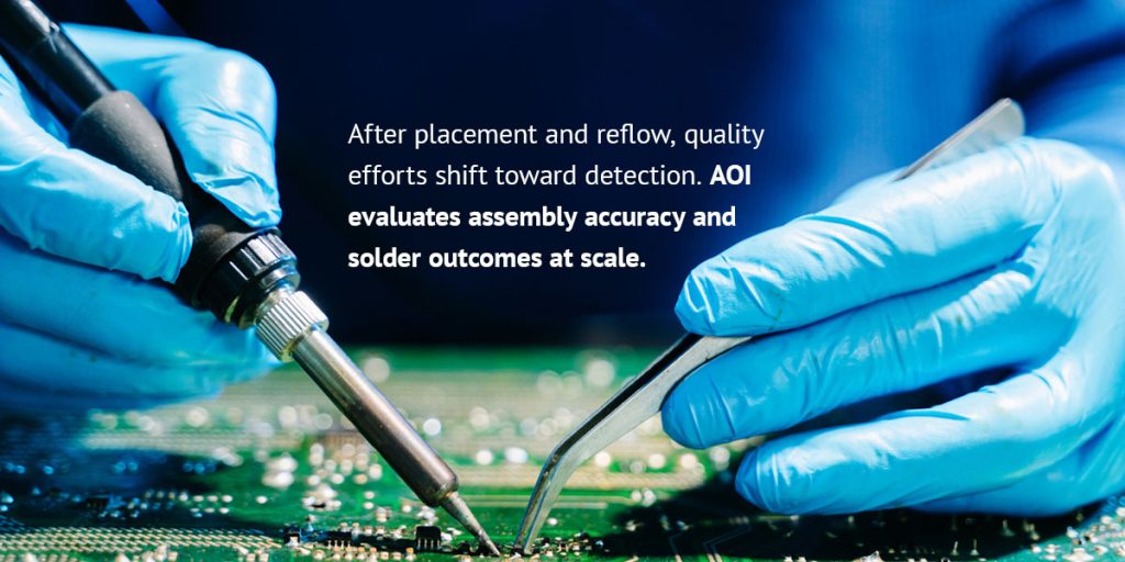
After placement and reflow, quality efforts shift toward detection. AOI evaluates assembly accuracy and solder outcomes at scale. It also helps teams identify issues that are difficult to detect manually, especially on dense designs.
1. Detecting Component Misalignment and Placement Errors
AOI uses imaging to compare assembled boards against design intent. These insights allow teams to correct process variation before it spreads.
Typical findings can include:
Skew and shift: Components moving during placement
Polarity errors: Orientation issues affecting function
Missing components: Placement interruptions
Tombstoning: Imbalance during reflow
2. Verifying Solder Joint Quality After Reflow
Beyond placement, AOI evaluates solder joint formation. Fillet shape, wetting behavior and consistency indicate whether joints meet PCB testing standards. This stage strengthens solder joint inspection by confirming mechanical and electrical readiness.
3. Improving Circuit Board Manufacturing Quality Through Consistency
Manual inspection remains valuable but introduces variability. Automated inspection provides repeatable evaluation across production volumes, improving circuit board manufacturing quality.
Functional Testing for Real-World PCB Assurance
Even when visual inspection appears correct, uncertainty can remain. Functional testing verifies whether the board performs as intended when powered and operating. This step represents the verification layer of quality assurance PCB strategies.
Moving Beyond Connectivity Checks
Connectivity confirms electrical paths. Functional testing confirms system behavior. As products become more complex, this distinction becomes increasingly important.
Simulating Real Operating Conditions
Functional testing recreates aspects of real use environments. These checks reduce late surprises and improve confidence before deployment.
Examples of simulating real use environments include:
Signal validation: Confirming logic behavior and outputs
Voltage response: Evaluating performance under load
Communication verification: Confirming protocol interaction, like CAN or I2C
Custom Fixtures and Software for PCB Testing Standards
Tailored fixtures and test routines ensure validation reflects real product requirements. As a result, testing aligns with engineering intent rather than generic pass criteria.
Statistical Process Control Methods for Continuous Improvement
Inspection shows what has happened. Statistical process control methods help prevent what might happen next. By analyzing SPI and AOI data over time, teams gain visibility into subtle variations that would otherwise remain unnoticed.
Using SPI and AOI Data to Monitor Process Stability
Trend monitoring helps teams intervene before defects appear. This approach can include paste volume drifting toward control limits, placement accuracy shifting across batches and reflow conditions affecting joint formation. Early visibility protects circuit board manufacturing quality.
Closed-Loop Feedback for PCB Defect Detection Prevention
A closed-loop system allows equipment adjustments based on inspection results. This process moves PCB defect detection from reactive correction toward proactive prevention.
Typical improvements are:
Printer adjustment: Correcting alignment and pressure
Placement tuning: Improving accuracy
Reflow optimization: Stabilizing solder quality
Quality Assurance PCB Assembly Is an Ecosystem
Quality control measures in PCB assembly are most effective when prevention, detection and verification operate together. This ecosystem supports more predictable launches, reduced rework and scrap, more substantial supplier confidence and improved field reliability. For teams managing complex electronics programs, a layered approach reduces uncertainty across the life cycle.
Choose Lectronix for Reliable Quality Control Measures in PCB Assembly
Minor manufacturing variations can create outsized risk. When those variations go unnoticed, they can delay validation, increase cost and affect product reliability after release.
Effective PCB quality assurance strategies address this challenge by integrating quality into the process rather than relying solely on late inspection. Combining SPI, automated optical inspection, functional testing and statistical process control creates a clearer path from prototype to production.
Working with Lectronix, a partner that integrates engineering, prototyping and assembly, can help your organization align these quality control measures, shorten feedback loops and support more confident product launches. Request a quote today for a quality-focused PCB assembly strategy.
Best Practices for PCB Design in Rugged Environments
Designing electronics to survive the real world is challenging. Conditions change, equipment vibrates and moisture finds its way into places it shouldn’t.
A board may perform well in testing but struggle once it moves into production or deployment. Rugged PCB design reduces that risk by shifting the focus from reactive to proactive. That means thinking carefully about materials, layout, mechanical support, environmental protection and how to validate the board before releasing it.
These PCB design best practices let you create boards that hold up under stress while keeping development timelines realistic and manageable.
PCB Design for Rugged Environments
Rugged PCB design starts with understanding the conditions the board will face during daily operation. The environment shapes material choices, layout decisions and protection strategies.
Designing a Vibration-Resistant PCB for Automotive and Industrial Applications
Vibration introduces continuous mechanical movement. Over time, that movement can weaken solder joints, shift connectors and create stress around heavier components.
Approaches for a vibration-resistant PCB include the following.
Board support strategy: Placing mounting points near heavier areas reduces flex during operation.
Component profile control: Lower profile components move less and place less strain on solder joints.
Balanced layout: Distributing mass across the board prevents localized stress.
Coping With Extreme Temperature Fluctuations and Thermal Shock
Temperature changes cause materials to expand and contract at different rates. Repeated cycling can lead to fatigue in solder joints, layer delamination and gradual performance degradation.
Temperature-resistant PCB design often involves selecting materials with compatible thermal properties and managing how heat moves across the board.
Resisting Moisture, Dust and Chemical Contaminants
Environmental exposure affects reliability in quieter ways. Moisture can lead to corrosion, dust can create leakage paths and chemical exposure can degrade protective layers.
Outdoor and industrial designs typically account for this through sealing strategies, protective coatings and connector choices that limit ingress without making the system difficult to service.
Understanding these environmental factors early makes later design decisions more intentional and reduces the likelihood of redesign.
PCB Material Selection for Ruggedized Circuit Board Design
Material influences how well a board holds up over time. Of course, electrical performance matters. However, mechanical stability and thermal behavior are central to reliability in harsh conditions.
The goal is to prevent issues that are difficult to correct later, such as warping, solder fatigue or layer separation.
High-Tg FR4 vs. Polyimide
High-Tg FR4 remains a common choice because it offers improved thermal stability compared to standard FR4 while maintaining cost efficiency. For many industrial applications, it provides a practical balance between performance and manufacturability.
Polyimide becomes more relevant when boards must tolerate higher temperatures, repeated thermal cycling or increased mechanical stress. Its flexibility and thermal resistance make it useful in designs where standard materials may fatigue over time.
Consider these material selection variables.
Thermal range: Higher glass transition temperatures support more stable operation during temperature cycling.
Mechanical behavior: Materials that resist cracking or flex fatigue extend product life.
Production scale: Some materials introduce longer lead times or additional manufacturing considerations.
Copper Weight and Plating Thickness for Durability
Copper structure influences electrical performance and mechanical strength. Heavier copper can improve current handling and reduce localized heating, while thicker plating strengthens pads and vias that experience stress.
Durable PCB design involves:
Increased copper weight for power distribution.
Reinforced vias in high-stress areas.
Plating strategies that reduce fatigue over time.
Component Placement and Mounting for Vibration Resistance
In rugged environments, component placement influences how the board handles movement, stress and long-term fatigue. A stable layout reduces the load placed on solder joints and connectors. It also makes validation more predictable because the board behaves consistently under vibration and mechanical shock.
Strategic Component Layout to Minimize Flex Stress
Boards naturally flex during operation, especially in vibration-heavy applications. Placement determines flex distribution. Design teams often focus on:
Positioning heavier components near mounting points
Avoiding high-mass clustering
Keeping sensitive components away from board edges
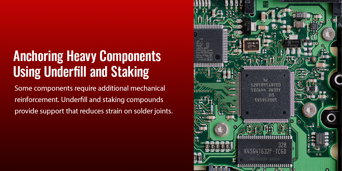
Anchoring Heavy Components Using Underfill and Staking
Some components require additional mechanical reinforcement. Underfill and staking compounds provide support that reduces strain on solder joints. These methods apply to connectors, large capacitors and components exposed to continuous vibration. They distribute stress more evenly and extend service life.
Selecting Rugged Connectors and Locking Mechanisms
Connectors experience repeated movement during operation and maintenance. Standard connectors may loosen over time, leading to intermittent failures that are difficult to diagnose.
Trace Routing and Thermal Management Strategies
Routing decisions influence more than signal integrity. In rugged applications, trace design affects heat distribution, mechanical durability and how the board responds to repeated stress.
Thermal buildup and localized stress often appear gradually. Routing that supports even heat flow and avoids vulnerable areas maintains performance over time. The objectives are consistency, stable temperatures, predictable current paths and reduced stress on critical interconnects.
Designing Power Planes for Effective Thermal Dissipation
Power planes spread heat across a larger area, preventing it from concentrating around individual components. It reduces thermal gradients that can accelerate material fatigue.
Strategies include:
Using larger copper areas to improve heat spreading and reduce hot spots.
Adding thermal vias beneath high-power components to move heat into inner layers.
Planning stackups with thermal behavior in mind for cooling and mechanical stability.
Trace Widths and Via Protection in High-Stress Zones
Trace geometry changes as boards flex and vibrate. Narrow traces are more susceptible to cracking, particularly near connectors or mounting areas. Designers often address this by increasing trace width in critical pathways, routing away from known flex zones and protecting vias through tenting or filling.
Outdoor PCB Design Best Practices — Protective Coatings and Enclosure Integration
In rugged applications, PCB design and enclosure strategy need to work together. Moisture, dust and chemical exposure don’t always cause immediate failure. The damage often builds slowly.
Conformal Coating and Potting for Environmental Sealing
Conformal coating creates a thin protective layer that shields board components and traces from moisture and contaminants while keeping the assembly serviceable. Potting provides superior protection by encapsulating components in a compound. It improves vibration resistance and environmental exposure but limits repairability.
Design Considerations for Sealed Enclosures
A sealed enclosure adds another layer of defense, but it also introduces thermal and pressure considerations. Internal heat buildup can shorten component lifespan if not managed correctly.
Design teams often coordinate on:
Ventilation or pressure equalization strategies
Gasket and sealing material selection
Mechanical support alignment
Testing PCB Design for Harsh Conditions
Validation confirms that design assumptions hold under real-world conditions. Early testing reduces the risk of field failures and redesign cycles.
Thermal Cycling and HALT HASS Testing Protocols
Thermal cycling evaluates material fatigue, while accelerated testing methods expose hidden weaknesses earlier in development. These approaches are common in ruggedized and mil-spec PCB design contexts, where reliability requirements are higher.
The Importance of Solder Paste Inspection for Joint Reliability
Solder paste inspection verifies paste volume and placement before reflow, improving solder joint consistency. Reliable joints are critical for vibration resistance and long-term durability, making SPI essential in rugged electronics manufacturing.
Building Rugged Electronics Without Slowing Innovation
Designing electronics for harsh environments means managing uncertainty. Engineers must deliver reliable products while working within tight schedules, complex supply chains and evolving performance expectations.
Thoughtful material selection, layout strategies, environmental protection and validation methods let teams create electronics that perform consistently in demanding conditions. It’s equally crucial to work with partners who understand engineering and production to reduce friction throughout development and protect time-to-market.
If you develop rugged electronics and want to streamline design, prototyping and production within a single integrated workflow, request a quote from Lectronix today and explore how a coordinated engineering and manufacturing approach can support reliable product development.
Electrical safety is a central concern in electronics manufacturing, where even minor oversights can have serious consequences. In these fast-paced environments, unique risks and specialized hazards demand a higher standard of awareness, preparation and ongoing commitment to diligent safety practices.
According to the U.S. Department of Labor, the U.S. manufacturing sector, including electronics manufacturing, experienced 391 fatal occupational injuries in 2023. Meeting and exceeding Occupational Safety and Health Administration (OSHA) standards is essential for protecting workers from industry-specific hazards.
The Hidden Dangers of Exposed Circuitry and Bare Boards
Electronic manufacturing environments involve rapid product changes, densely packed boards and frequent manual intervention. These factors increase exposure to live circuitry, micro-scale faults and hard-to-predict hazards.
One of the most overlooked risks comes from stored-energy components, such as capacitors. Even when power is completely disconnected, capacitors can retain a dangerous charge long after shutdown. During safety checks, rework or late-stage assembly, technicians reaching for one of these boards may inadvertently encounter voltage levels strong enough to cause severe injury.
Adding to the challenge, “hot” testing environments require technicians to work directly with energized systems. This necessary step in quality control exposes staff to potential arcs, shocks and sudden malfunctions, demanding specialized procedures and continuous vigilance beyond conventional electrical safety standards.
The Effect of Electrical Shock on the Human Body
The effect of electric shock on the human body can range from unnoticeable to fatal, depending on the amount of current that flows. Several factors affect the amount of current a human body experiences, including sweat level and shoe selection. Due to such differences, two people touching an identical voltage may have entirely different experiences. In mild cases, electrical shock can result in mild tingling, while higher voltage shocks can result in internal organ damage and cell breakdown or death.
Identifying Key Electrical Hazards in Assembly Environments
Assembly lines present a range of unique electrical hazards that require targeted attention, with risks stemming from both the manufacturing environment and the inherent complexity of the devices produced. Key safety hazards in electrical engineering include:
Electrical shock: When a human body becomes part of the electrical circuit, the person will experience an electrical shock. This shock can result in a range of injuries, from minor discomfort to death.
Arc flash: An arc flash is a rapid release of energy due to an arcing fault. This hazard occurs during short circuits in high-power test fixtures and can result in violent explosions, fires and severe burns.
Electrostatic discharge (ESD): There is a misconception that ESD gear protects workers. In reality, gear like grounding wrist straps is for product safety, not personnel safety.
Improper grounding: Improper grounding is a serious hazard. When a circuit lacks a path to the ground, it will find an alternative path, which could involve jumping to another live component or passing through a worker.
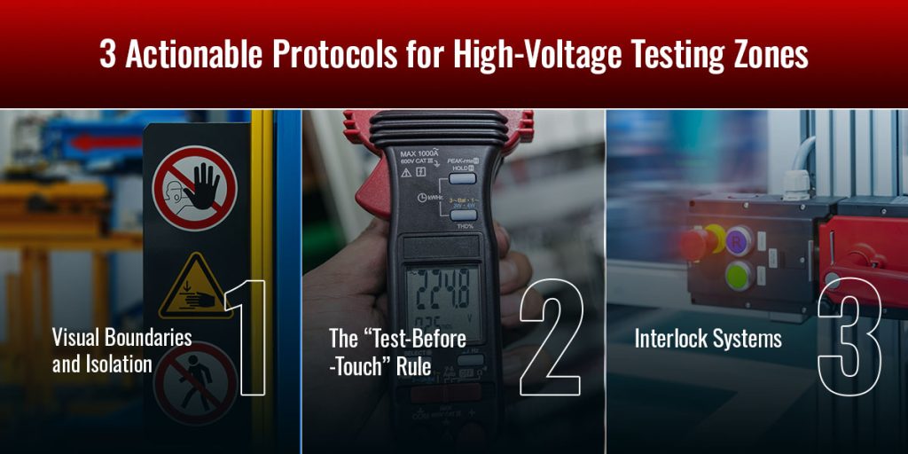
3 Actionable Protocols for High-Voltage Testing Zones
Effective high-voltage testing demands proactive steps to minimize risk and safeguard workers. The following protocols significantly reduce exposure to electrical hazards in these specialized areas:
1. Visual Boundaries and Isolation
Marking hot testing areas requires isolating the station, installing proper signage and using floor markings. Signage should specify voltage levels and indicate that only authorized personnel can be in the area. Use specific colors to indicate warnings or danger levels. These visual boundaries are critical to alerting staff and visitors to elevated risk and help ensure that only authorized, properly equipped personnel can enter these areas during live testing procedures.
2. The “Test-Before-Touch” Rule
This rule requires workers to ensure that electrical equipment is de-energized before touching it. Testing means checking equipment with properly rated voltage testers and, for high-capacitance boards, using approved discharge sticks to ensure no potentially lethal stored charge remains even when the system appears powered down. Embedding this disciplined approach into standard operating procedures dramatically reduces the risk of accidental electric shock and enforces a culture of vigilance.
3. Interlock Systems
Automated interlock systems and electromechanical safety devices are a critical layer of protection for high-voltage test fixtures. These safety mechanisms should instantly disconnect power if a worker opens an enclosure or access panel. This process is designed to make the device safe to touch. By removing human error from the equation, interlock systems aim to prevent accidental exposure to hazardous voltages and promote a safer testing environment. For best results, teams should regularly test these systems and implement maintenance to ensure reliable functionality on every use.
Essential PPE and Training for Electronics Personnel
Protecting electronics personnel goes beyond basic awareness. Safe workplaces require the right personal protective equipment (PPE) and provide a foundation of practical, hands-on safety training tailored to the unique hazards found in this industry.
Targeted Protection: Protective Equipment Relevant to Electronics
Choosing the proper PPE is essential for ensuring safety in the electronics industry, where specialized gear can mean the difference between minor incidents and serious injury during electrical work. Critical PPE includes:
Voltage-rated gloves: Cotton assembly gloves are not adequate for working with high voltages. Choose insulated gloves that are easy to work with.
Safety glasses with side shields: Face and head equipment is critical. Face shields and safety glasses protect workers from arc flashes and intense heat.
Flame-resistant (FR) clothing: For applications where arc flash is a risk, FR clothing is critical for reducing risk. You can also find FR aprons and smocks for added protection.
Safety boots: Workers should wear footwear that does not conduct electricity. Sturdy leather or rubber boots can reduce slipping risks and protect workers from electrical hazards.
Competency-Based and Hands-On Training
Maintaining electrically safe work conditions requires teams to adopt a practical learning approach that demonstrates employee competency and allows workers to gain practical experience with electrical applications. OSHA electrical safety standards require employees who face shock risks to complete training to recognize, avoid and mitigate electrical risks. However, classroom instruction alone is not enough. Truly effective training should include hands-on exercises, real-world simulations and regular skill assessments to ensure workers can apply safety protocols in practice.
Ongoing, competency-based training helps reinforce critical concepts and adapts as technology changes, enabling teams to respond confidently to new or unexpected hazards. Integrating hands-on elements into your safety guide for electronic products ensures that employees understand and can perform the procedures necessary to maintain a safe work environment. This practical approach builds lasting safety habits, reduces errors and keeps both personnel and products protected on the job.
Lockout/Tagout (LOTO) for Maintenance
The Lockout/Tagout (LOTO) procedure is a safety practice for protecting workers during machine maintenance. Proper procedures follow these steps:
Preparation: Authorized employees must identify specific hazards and understand how to control hazardous energy.
Shutdown: Teams shut down the equipment or machine that will undergo servicing.
Isolation: Workers must isolate the equipment, which could involve shutting a valve, turning off power at a breaker or something else.
LOTO: An authorized worker attaches a lockout/tagout device to each isolated machine. These devices prevent unexpected equipment startup and include tags with the name of the person performing the lockout and other relevant information.
Stored energy check: Workers inspect the equipment for residual energy that could cause harm if unreleased.
Isolation verification: An authorized employee double-checks that the machine is isolated and de-energized.
Maintain Electrical Safety in the Workplace
Adhering to rigorous safety protocols protects your workforce and safeguards product integrity. Proactive measures, hands-on training and proper equipment are essential for minimizing risk and maintaining a culture of vigilance. By partnering with experts like Lectronix, Inc., you gain access to advanced manufacturing solutions and experienced teams who prioritize safety at every step.
Lectronix, Inc. is a leading supplier of electronic hardware and software technology. We’re committed to delivering quality and security in every project. Our electronic manufacturing services include:
Logistics
Prototyping
PCB assembly
Mass production
Systems assembly
Inspections and testing
New product introduction
Allow us to assist you with electronic innovations. Protect your people, ensure your product’s performance and build lasting success with a manufacturing partner that puts safety first. Contact us for a personalized quote.
The Future of Police Vehicle Computing and Mobile Devices
Officers are managing multiple disconnected systems with separate laptops, stand-alone radios and independent control panels, all competing for available dashboard space. Modern law enforcement requires a different approach.
The future of police vehicle computing centers on a unified mobile command center built on integrated control systems, rugged mobile devices and real-time connectivity. This guide explores the key technologies and strategic considerations for transforming your fleet with advanced electronic solutions tailored to 21st-century law enforcement demands.
The Modern Patrol Vehicle: A Unified Mobile Command Center
The most advanced police departments are reimagining their patrol vehicles as mobile command centers where every system communicates effectively.
From Siloed Systems to an Integrated Digital Hub
Today’s leading patrol vehicle designs consolidate communications equipment into a unified interface that gives officers access to all critical functions through a single touch point. A police vehicle computer built on integration principles eliminates the complexity of managing multiple separate devices.
Integrated digital hubs offer significant operational advantages and enhance the user experience for officers in several ways:
Drivers can access information on a single display rather than shifting their attention across multiple screens.
Streamlined interfaces reduce fatigue during extended shifts and simplify training for new officers.
Unified data access means faster response times in time-critical situations.
Single integrated systems reduce the complexity and cost of fleet-wide technology support.
The integrated digital hub approach advances beyond traditional mobile data computers (MDCs) and land mobile radios (LMRs) by creating a truly unified platform, where systems work in concert rather than operating independently.
Core Capabilities of the Next-Generation Police Vehicle
Modern integrated patrol vehicles deliver capabilities that transform how officers perform their daily duties:
Seamless real-time data access that keeps officers informed with instant access to databases, mapping systems and dispatch information.
Multi-source video integration that brings together body cameras, dashboard cameras and drone feeds.
Cross-agency communication that’s built on interoperability standards that enable simplified coordination during joint operations.
Edge-based data processing that analyzes information within the vehicle for faster decision-making and continued operation during network interruptions.
Officers equipped with comprehensive information make better tactical decisions.
Four breakthrough technologies enable the shift toward fully integrated mobile command centers.
5G and Resilient Connectivity (FirstNet)
The high bandwidth and low latency of 5G networks enable police departments to handle massive data flows, including high-definition video, real-time license plate recognition and continuous database queries. FirstNet takes this foundation further by providing a dedicated public safety network designed to provide priority connectivity during major events when commercial networks become congested.
The public safety 5G market is projected to reach $6.3 billion by 2028, underscoring the critical role of resilient connectivity in modern law enforcement. Real-world deployments demonstrate the operational value. City managers are tapping FirstNet for interoperability, connectivity and cost savings, successfully streaming body camera video and connecting mobile data terminal police systems with reliable connectivity.
Rugged Mobile Devices
Purpose-built ruggedized devices deliver the durability law enforcement environments demand. These mobile devices are typically manufactured to military standards to withstand the constant vibration, extreme temperatures and physical impacts encountered during daily operations.
They can provide:
Superior sunlight readability for viewing information in bright daylight conditions.
Reliable vehicle integration with secure mounting and dependable power and data connections.
An extended operational lifespan that reduces the total cost of ownership across the fleet life cycle.
Field-proven durability that supports officer connectivity across various conditions.
The shift toward purpose-built ruggedized tablets and displays reflects a strategic recognition that patrol vehicle environments require engineering specifically designed for these unique demands.
Real-Time Analytics and Automated License Plate Readers (ALPRs)
Edge computing processes data within the vehicle rather than sending everything to remote servers for analysis. This architecture delivers significant performance and reliability advantages.
Processing happens locally, which dramatically improves response times, and systems can continue to function during periods of reduced network connectivity.
ALPRs demonstrate the practical value of AI in modern patrol vehicles. Advanced machine learning and computer vision enable ALPR systems to analyze much more than license plates, including detecting vehicle dents, identifying specific bumper stickers, processing specialty tags and recognizing rideshare logos.
The most sophisticated ALPR platforms deliver comprehensive capabilities, including:
Automated plate reading that processes images and determines vehicle make, model, color and year.
Hot list comparison that checks plates against local and national databases in real time.
Routing that makes intelligent predictions about probable vehicle travel routes.
Localized alerts that notify law enforcement units in the area when matches occur.
Automated reporting that generates vehicle activity reports and improves future system accuracy through ongoing analysis.
Integrated In-Vehicle Computing (IVC)
All these advanced technologies require a powerful central platform to orchestrate their operation. The Integrated Control System (ICS) serves as the intelligent hub managing 5G modems, AI processing modules, rugged displays and legacy equipment integration.
A robust IVC platform enables the consolidation of audio, video and controls into a single, manageable interface. This central computing platform is where the vision of a unified mobile command center becomes an operational reality.
A Strategic Roadmap to Creating Your Fleet’s Future
Transforming your patrol fleet requires thoughtful planning and strategic decision-making. Three key considerations guide successful modernization efforts.
1. Assess Your Current Capabilities and Technology Gaps
A comprehensive technology audit creates the foundation for smart investment decisions. Engage directly with officers to gather frontline insights about operational challenges. The most valuable assessment questions include:
What daily tasks take longer than they should due to technology limitations?
Which systems currently operate in isolation rather than sharing data?
Where do officers experience the greatest frustration with existing equipment?
What capabilities do neighboring departments have that would benefit your operations?
A data-driven approach to fleet management enables you to prioritize improvements based on operational impact. Document current capabilities, identify specific gaps and build a clear picture of where modernization delivers the greatest value.
2. Determine the “Buy vs. Build” Decision
Police departments can choose between purchasing off-the-shelf original equipment manufacturer (OEM) vehicles or partnering with specialized engineering firms to create custom, deeply integrated solutions. Both paths offer distinct advantages depending on your specific requirements.
Ford Police Interceptor Utility vehicles and similar OEM offerings integrate more technology with each model year. These standardized platforms provide predictable specifications and established support networks.
Custom engineering partnerships offer an alternative for departments seeking maximum control, flexibility and future-proofing. Specialized firms offering turnkey product development solutions can integrate systems more deeply than standard OEM configurations.
The custom-engineering approach requires a greater up-front investment. But agencies with unique requirements or long-term strategic technology visions often find that this path provides superior long-term value.
3. Prioritize Scalability and Future-Proof Your Investment
Technology evolves continuously. The systems your department invests in today should accommodate emerging innovations. Miami-Dade County, Florida’s deployment of the nation’s first autonomous patrol vehicle in October 2025 illustrates how rapidly new capabilities are arriving. Modular, scalable architecture protects your investment by enabling your platform to evolve alongside these advancements.
Evaluate potential solutions based on their upgrade paths. Look for platforms that allow new capabilities to be added through software updates, and prioritize hardware components built on industry-standard interfaces that accommodate future peripherals. Consider vendors offering long-term strategic partnerships that evolve alongside your needs.
The goal is to select systems designed for evolution. Forward-thinking departments prioritize platforms built on open standards and modular designs that grow alongside technological advancement.
Partner With Lectronix to Build Your Next-Generation Fleet
The future of police vehicle computing hinges on creating a single, integrated digital hub that unifies data access, communications and control systems. Achieving this vision requires a partner with deep expertise in both hardware and software engineering.
Lectronix delivers turnkey product development solutions that transform complex technical requirements into fully integrated, field-ready systems. Our U.S.-based engineering and manufacturing capabilities enable us to develop state-of-the-art rugged displays, custom control platforms and complete vehicle integration packages tailored to your specific operational needs.
Welcome to our new website! We have revamped the entire site with goal of better describing our company and the unique combination of electronics services, technologies, and products we offer. The entire site should be more friendly for browsing by mobile devices. Many times visitors to our facility have said something along the lines of “wow! you do some really cool things here that I wouldn’t have guessed” and part of our effort has been to make some of our cutting-edge R&D technology development more apparent on the web. We also wanted to introduce this blog as a place for us to discuss hot topics in electronics development and manufacturing. So if you purchase, develop, or even just are interested in electronics, come back as we’re sure you’ll find interesting information here in the future!