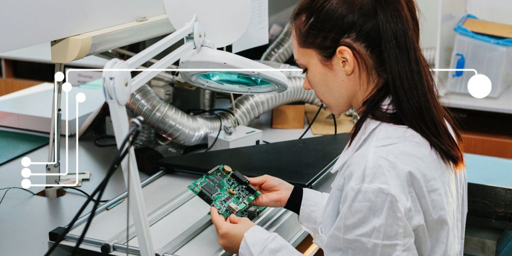
Quality Control Measures in PCB Assembly
Product launches carry pressure long before anything ships. Engineering teams are balancing timelines, performance requirements, supplier coordination and the constant concern that a minor manufacturing issue could create a much larger problem later.
In printed circuit board (PCB) assembly, that risk often comes from defects that are difficult to see early. A slight variation in solder paste or a component that shifts during placement can lead to rework, delayed validation, field failures and uncomfortable conversations about reliability. Teams know quality control matters. The challenge is understanding which measures actually prevent defects rather than simply catching them after the fact.
Below, we discuss the quality control measures used in PCB assembly to reduce risk across the build process. We also cover AOI automated optical inspection, functional testing, solder joint quality assessment, defect-prevention strategies, and statistical process control methods, so teams can make more confident manufacturing decisions.
Why PCB Assembly Quality Control Standards Matter
PCB assembly quality control involves meeting specifications and creating consistency across builds. The goal is to ensure performance remains predictable as volumes increase. When processes are stable, teams spend less time troubleshooting variability and more time advancing products.
The Hidden Defect Risk in Circuit Board Manufacturing Quality
A board can pass electrical checks and still carry risk. Environmental stress, extended operating hours and system integration often expose issues that were not visible during early validation.
The following examples are the kinds of issues that make circuit board manufacturing quality a process challenge rather than a final inspection task:
- Micro-voids in solder joints, which can reduce long-term mechanical reliability
- Slight component skew that affects signal performance and tolerance margins
- Paste variation, which creates intermittent failures that appear later
The Inspection Misconception in Quality Assurance PCB
Many teams assume that inspection at the end will catch problems. In reality, late detection increases cost and slows progress. Quality assurance PCB strategies work best when they focus on controlling inputs, monitoring variation and identifying drift before defects appear.
A Defense-In-Depth Approach to PCB Testing Standards
Practical PCB testing standards follow three connected layers:
- Prevention: Stabilizing critical inputs like solder paste
- Detection: Identifying placement and solder issues during assembly
- Verification: Confirming real product behavior
This defense-in-depth approach forms the backbone of modern quality control measures in PCB assembly.
The Foundation of PCB Defect Prevention
Solder paste inspection (SPI) occurs at the beginning of the assembly process, where many defects originate. Because paste defines every electrical and mechanical connection, minor inconsistencies can affect the entire build. SPI shifts quality earlier by identifying variation before components are placed.
Preventing Defects Before Component Placement
Paste volume and alignment directly influence solder joint integrity. When the paste is incorrect, later processes cannot fully compensate. A few common issues that may be detected include insufficient paste, excess paste and paste misalignment. Addressing these conditions early reduces rework and protects downstream yield.
3D Measurement for High-Reliability PCB Assembly Quality Control
Modern SPI systems capture detailed measurements of paste deposits, including volume, height and area. This data provides visibility into print consistency across the entire board.
By stabilizing the printing process, teams strengthen the foundation of PCB assembly quality control. Key benefits of 3D measurement include:
- Volume verification: Supports electrical reliability across runs
- Height consistency: Improves placement accuracy
- Area coverage: Confirms proper pad engagement
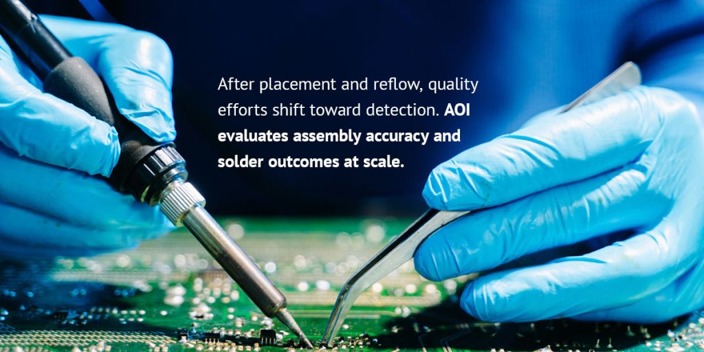
Automated Optical Inspection (AOI) in PCB Inspection Methods
After placement and reflow, quality efforts shift toward detection. AOI evaluates assembly accuracy and solder outcomes at scale. It also helps teams identify issues that are difficult to detect manually, especially on dense designs.
1. Detecting Component Misalignment and Placement Errors
AOI uses imaging to compare assembled boards against design intent. These insights allow teams to correct process variation before it spreads.
Typical findings can include:
- Skew and shift: Components moving during placement
- Polarity errors: Orientation issues affecting function
- Missing components: Placement interruptions
- Tombstoning: Imbalance during reflow
2. Verifying Solder Joint Quality After Reflow
Beyond placement, AOI evaluates solder joint formation. Fillet shape, wetting behavior and consistency indicate whether joints meet PCB testing standards. This stage strengthens solder joint inspection by confirming mechanical and electrical readiness.
3. Improving Circuit Board Manufacturing Quality Through Consistency
Manual inspection remains valuable but introduces variability. Automated inspection provides repeatable evaluation across production volumes, improving circuit board manufacturing quality.
Functional Testing for Real-World PCB Assurance
Even when visual inspection appears correct, uncertainty can remain. Functional testing verifies whether the board performs as intended when powered and operating. This step represents the verification layer of quality assurance PCB strategies.
Moving Beyond Connectivity Checks
Connectivity confirms electrical paths. Functional testing confirms system behavior. As products become more complex, this distinction becomes increasingly important.
Simulating Real Operating Conditions
Functional testing recreates aspects of real use environments. These checks reduce late surprises and improve confidence before deployment.
Examples of simulating real use environments include:
- Signal validation: Confirming logic behavior and outputs
- Voltage response: Evaluating performance under load
- Communication verification: Confirming protocol interaction, like CAN or I2C
Custom Fixtures and Software for PCB Testing Standards
Tailored fixtures and test routines ensure validation reflects real product requirements. As a result, testing aligns with engineering intent rather than generic pass criteria.
Statistical Process Control Methods for Continuous Improvement
Inspection shows what has happened. Statistical process control methods help prevent what might happen next. By analyzing SPI and AOI data over time, teams gain visibility into subtle variations that would otherwise remain unnoticed.
Using SPI and AOI Data to Monitor Process Stability
Trend monitoring helps teams intervene before defects appear. This approach can include paste volume drifting toward control limits, placement accuracy shifting across batches and reflow conditions affecting joint formation. Early visibility protects circuit board manufacturing quality.
Closed-Loop Feedback for PCB Defect Detection Prevention
A closed-loop system allows equipment adjustments based on inspection results. This process moves PCB defect detection from reactive correction toward proactive prevention.
Typical improvements are:
- Printer adjustment: Correcting alignment and pressure
- Placement tuning: Improving accuracy
- Reflow optimization: Stabilizing solder quality
Quality Assurance PCB Assembly Is an Ecosystem
Quality control measures in PCB assembly are most effective when prevention, detection and verification operate together. This ecosystem supports more predictable launches, reduced rework and scrap, more substantial supplier confidence and improved field reliability. For teams managing complex electronics programs, a layered approach reduces uncertainty across the life cycle.
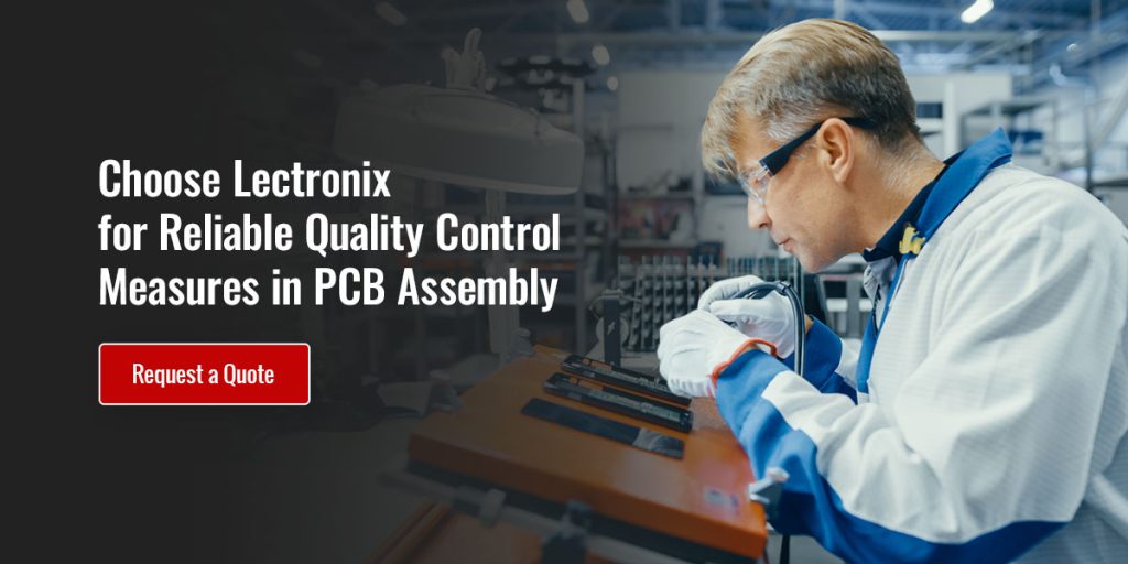
Choose Lectronix for Reliable Quality Control Measures in PCB Assembly
Minor manufacturing variations can create outsized risk. When those variations go unnoticed, they can delay validation, increase cost and affect product reliability after release.
Effective PCB quality assurance strategies address this challenge by integrating quality into the process rather than relying solely on late inspection. Combining SPI, automated optical inspection, functional testing and statistical process control creates a clearer path from prototype to production.
Working with Lectronix, a partner that integrates engineering, prototyping and assembly, can help your organization align these quality control measures, shorten feedback loops and support more confident product launches. Request a quote today for a quality-focused PCB assembly strategy.